About a decade ago, I joined the ranks of a forward-thinking company, not just a player in the IoT space but a creator of custom industrial mobile devices and solutions. With a background steeped in app development and a knack for unraveling complex systems, I was entrusted with leading our Solutions of Connected Devices unit. Our ambition was to craft a seamless fusion between the finesse of app development and the concrete realities of intricate device engineering. We weren’t just connecting devices to the cloud—we were delving into their very core, understanding each component’s role in our expansive industrial Mobile Devices and IoT ecosystem. Despite my seasoned analytical skills, the depths of mobile device engineering were new terrain. Then came the pivotal turn in my journey, a discovery that would bridge my gap in understanding—the insightful teardowns on iFixit. This platform peeled back the layers of device complexity, turning the arcane into the accessible and marking the start of an era of clarity for me.
The Initial Struggle with Device Innards: The Teardown Revelation
When I ventured into the realm of mobile devices, the complexity was daunting. My established skills in app development didn’t quite translate to the intricate webs of electronics I encountered. The pace of learning was slow, and I could feel frustration knocking at my door.
That’s when I discovered iFixit, a device repair go-to-site, and with it, a critical shift in my learning process. The site’s teardowns provided a roadmap to understanding—each component’s role suddenly made sense. It was a breakthrough, a lens through which even the most complex devices became decipherable.
The clarity that iFixit’s teardowns provided resonated with my mechanical engineering roots. The hands-on experience of designing and manufacturing mechanical systems instilled in me a way of learning through tangible interactions. Despite my initial aversion to the abstract nature of electronics, I found myself drawing on this tactile understanding to demystify the once-intangible electronics of mobile devices.
Glimpse into the Heart of Innovation: Teardowns of the Titans
As I navigated through the complexities of device engineering, the teardowns of the Samsung Galaxy S5 and iPhone 5 provided invaluable insights, offering a detailed look into the ingenuity of these industry titans.
The Benefits of the Teardown Learning Approach
Teardowns turned out to be an educational goldmine. Here’s why:
- Demystifying Technology: Teardowns helped demystify the electronics that had seemed so abstract. Seeing each component, understanding its purpose, and how it fits into the larger system was incredibly enlightening.
- Hands-On Experience: Even though I wasn’t physically dismantling devices, the detailed guides gave me a virtual hands-on experience, which is the best way to learn.
- Systems Thinking: Approaching devices as systems to be broken down and analyzed improved my understanding of how the parts of IoT devices interact, which is essential for systems thinking.
- Cross-Disciplinary Insights: The process bridged my mechanical engineering knowledge with electronics, giving me a holistic view of product design and function.
- Enhanced Problem-Solving: Understanding the individual components and their interrelationships within a device sharpened my problem-solving skills, which is crucial for developing IoT solutions.
- Innovation Inspiration: Seeing the inner workings of various devices sparked ideas for innovation in my own projects, as I began to understand what was possible.
Conclusion: Connecting the Dots
In hindsight, the path from confusion to clarity in IoT device engineering was an adventure. The teardown approach played a pivotal role in translating my skills in mechanical engineering and app development to the world of connected devices. It taught me that sometimes, to build or innovate, we must first take things apart to understand them. And this has been an invaluable lesson as I continue to contribute to solutions in different fields.
Contrarian Views – Dissecting the Teardown Method: A Critical Perspective
While virtual teardowns offer a unique educational perspective, they are not without their detractors. Here are some potential contrarian views on the teardown approach to learning:
- Lack of Hands-On Experience: Critics argue that watching teardowns cannot replace the tactile learning experience that comes from physically handling the devices.
- Overemphasis on Disassembly: There’s a belief that teardowns may overemphasize the disassembly process without equally stressing the reassembly, which is crucial for actual repair and engineering understanding.
- Risk of Misinformation: The information from a virtual teardown can sometimes be misleading if not accompanied by expert commentary, leading to misconceptions about device functionality.
- Dependence on Interpretation: The learning is heavily dependent on the interpreter’s knowledge; without a deep understanding, viewers may miss out on crucial details.
- Inaccessibility of Tools: Teardowns often require specialized tools and knowledge that the average viewer may not have, which could limit the learning experience.
- Potential for Intellectual Property Issues: Some argue that teardowns could inadvertently expose proprietary techniques and designs, leading to intellectual property concerns.
- Oversimplification of Complex Systems: There’s a viewpoint that virtual teardowns oversimplify the complexities of modern devices, potentially overlooking the nuances of electronic design.
- Variability in Quality: The educational value of a teardown is only as good as its presentation, and there can be significant variability in the quality of information provided.
- False Confidence in Repair Ability: Observing teardowns might give untrained viewers a false sense of confidence in their ability to repair or tamper with devices, which can lead to further damage.
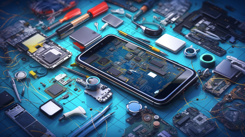
MidJourney Prompt with inputs from ChatGPT
Create an image of a modern engineer’s workspace during a teardown analysis of an IoT device. The scene is set in a well-lit room. On the desk, there’s an organized chaos of engineering tools – precision screwdrivers, a digital multimeter, a soldering iron, and a magnifying glass stand out. In the center, a smartphone is disassembled, its parts meticulously arranged: the screen, battery, circuit boards, and screws are visible. To one side of the desk, there’s a laptop displaying the iFixit teardown guide for the device, with visible tabs and diagrams. Surrounding the laptop and device parts, there are handwritten notes and electrical schematics, illustrating a moment of intense concentration and discovery. The overall atmosphere is one of focused innovation, blending traditional engineering with cutting-edge technology. –ar 16:9